High accuracy die placement requires precise magnification and resolution. It is nearly impossible to achieve sub-micron placement without accurate use of both of these elements.
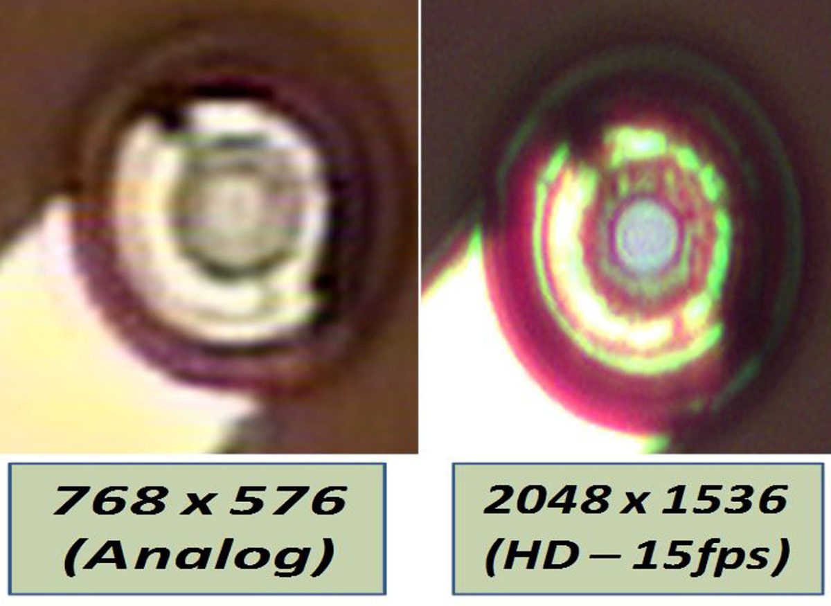
Alone, high magnification provides a lot of magnification, but the result will produce an image that becomes blurry (magnifying a signal with noise). In most cases, high accuracy will not be repeatable or achievable.
Now, flip it and you have excellent resolution but minimal magnification. Without the addition of high magnification, it is nearly impossible to achieve high accuracy die placement because often times the images used for alignment are so small. A good example of this is Optoelectronic bonding. Imagine aligning and placing a VCSEL or Photo Diode device, where the aperture is only 12 microns in diameter. How is it possible to achieve >1 micron accuracy if the field of view (FOV) is measured in millimeters? The answer is, its very difficult, if not impossible.
High magnification combined with high resolution provides the sharp image for alignment needed to achieve high placement accuracy. Finetech bonders use highest quality optics technology to provide the precise magnification and resolution needed for today’s advanced, sub-micron devices.
11/04/2014, created by: Robert Avila

