Standardized Indium Bump Interconnect/Hybridization Process for IR Sensor Assembly
Schedule an appointment with our experts
Standardized Process for IR Sensor Assembly
Talk to our experts

Is your goal to produce large format, high density infrared thermal imaging sensors that meet today's industry requirements?

Is your goal to produce large format, high density infrared thermal imaging sensors that meet today's industry requirements?

Due to the beneficial characteristics, the preferred way of hybridization to build IR thermal imaging sensors is by using fine pitch micro Indium bump array interconnect bonding. However, industry specialists are frequently pointing to very specific challenges associated with Indium bump bonding.

The challenges most frequently stated tend to be excessive preparation times, caused by lengthy machine setup and programming, material cleaning and co-planarity adjustment, trouble with inconsistencies in the bonding process, again due to lacking co-planarity and surface flatness, and a generally high complexity in maintaining yield and throughput impacted by insufficient bonding results. As a result, bonding processes are not automated, inconsistent, and manufacturing time and costs increase.

In order to tackle these challenges and provide the industry with an easy-to-use, efficient and reliable solution, Finetech has developed  standardized Indium bump interconnect/hybridization processes:

  • Fully Automated Indium bonding process, four or more assemblies per cycle
  • Cold Compression bonding up to 1000N
  • Thermal Compression bonding below 100°C
  • Formic Acid Indium oxide reduction below 220°C + Cold/Thermal Compression Bonding in an inert gas environment
  • Formic Acid reflow bonding down to 0.05 N PID Force controlled bond

Available for both semi-automated and fully automated die bonder systems!

Finetech hybridization process solution for IR sensor devices

From first sample to successful bonding in less than 6 hours

The Indium bump-to-bump die bonding is probably the most challenging part of thermal imaging IR sensor bonding/hybridiziation. We offer standardized hardware and process solutions for everything from manual to fully automated bonding, cold, thermal or formic acid reflow bonding and we can help you get your processes up and running within 6 hours.

Consistent 99%+ pixel yield

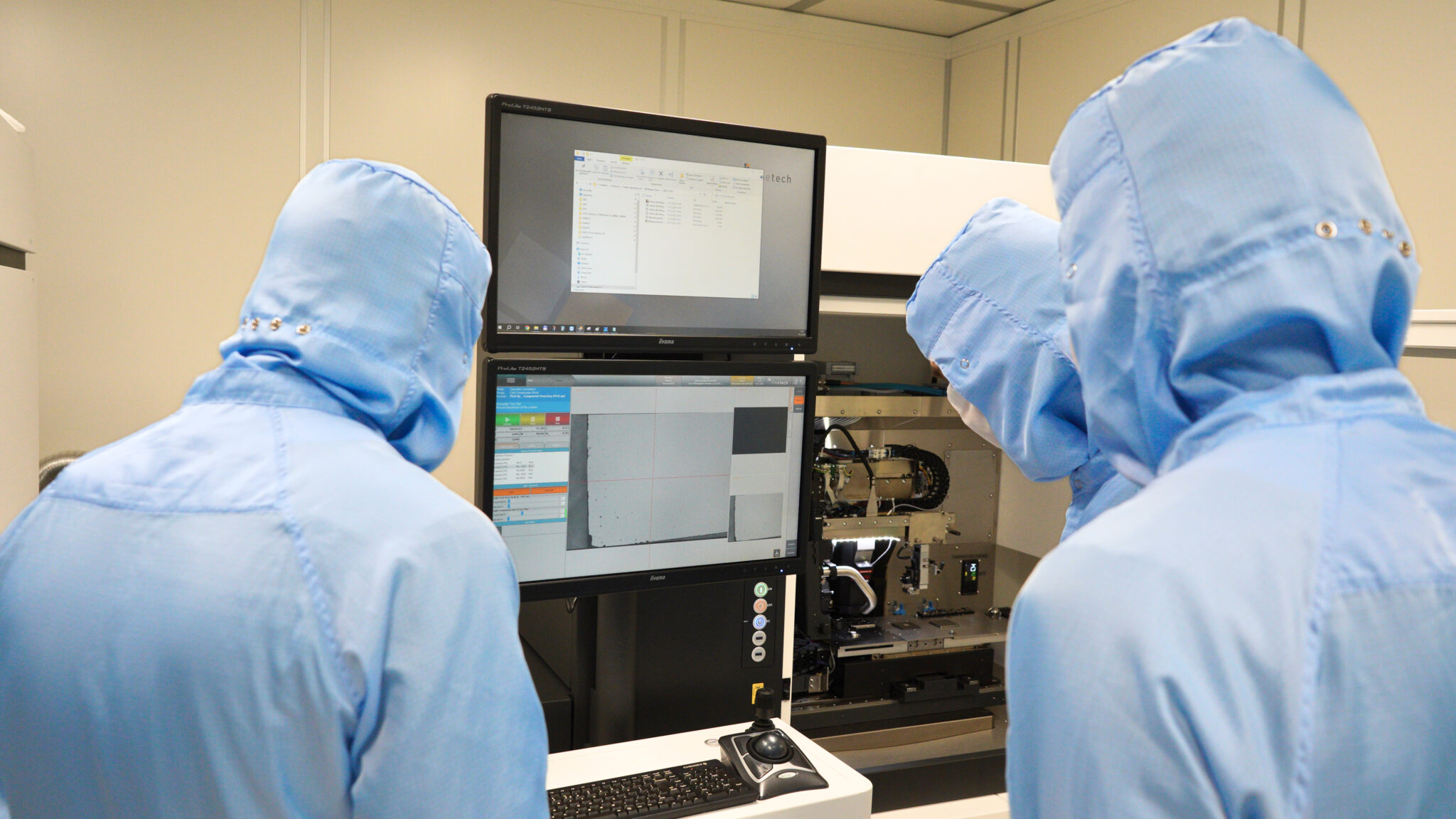
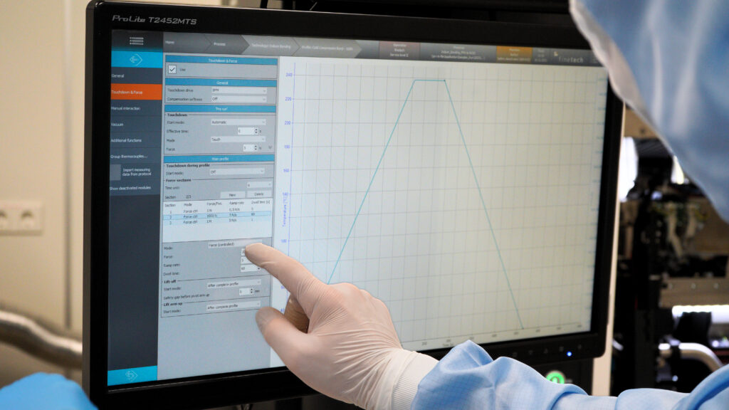
Consistency in parameters and their execution such as accuracy, force, time, and temperature ensures uniform, reliable and repeatable bonding quality across large pixel arrays and multiple assemblies. By accomplishing this 99%+ pixel yield consistency even on 640x512 SWIR sensors and more, our solution allows you to push the envelope of how your IR sensor devices is able to perform.

Cryogenic IR imaging applications

Our solution gives you access to cold compression bonding, the ideal way to address the issue of CTE mismatch in cryogenic IR imaging applications

Our solution in detail

number-one

Tweezer-safe handling and cleaning kit

Stand-alone material cleaning and preparation kit for tweezer-safe die handling, as well as chemical cleaning of photoresist and formic acid oxide reduction on Indium bumps.

number-2

Sub-micron flatness and co-planarity

<1 µm flatness and co-planarity on both heated and cold die handling and bonding surfaces, as well as – <1 µm passive tool leveling for co-planarity in bondline thickness.

number-3

Up to 50 nanometers alignment accuracy

Achieve sub-micron bump-to-bump post-bond alignment of 350K+ Indium Interconnects.

number-four

Precision temperature management

Our die handling and bonding surfaces heat up up to 450°C. The solution is able to keep within <1K temperature control. Maintaining precise temperature prevents thermal stress on bond and sensor die.

number-5

Controlled bonding environment

Prevents contamination that could compromise co-planarity, bond line gap, alignment and mechanical or electrical connectivity. We offer Nitrogen (N2) and Formic Acid bonding environments within a closed cell die bonder.

six

Fully automated bonding

Fully automated die bonding process with automated system calibration to ensure highest process repeatability.

Cleaning Station

Cleaning Station?

Our technical paper provides an insight to the technology behind infrared thermal imaging FPA sensors, including their operating principles, construction, and applications, as well as the challenges and their solutions in the IR FPA flip chip compression die bonding process.
e7025f48-b4bd-4c86-abde-9555d1dc32b7

Talk with our experts

Setting up a new indium bump-to-bump process? Need some support to reduce development time and costs? Book a 45-minutes consulting session free of charge with our product and application specialists to discuss how our solution can help you to optimize your processes.

Michael Wolf

Head of Application

Martin Rogge

Head of Product Management

Travis Scott

Business Development

*depending on system and configuration

Schedule a session with our experts

Contact Us

If you have a service request, please click here.

此栏为必填项。
此栏为必填项。
此栏为必填项。
此栏为必填项。
此栏为必填项。
此栏为必填项。
此栏为必填项。
此栏为必填项。
此栏为必填项。
此栏为必填项。
此栏为必填项。
此栏为必填项。
此栏为必填项。
此栏为必填项。
此栏为必填项。
此栏为必填项。
此栏为必填项。
此栏为必填项。
此栏为必填项。
此栏为必填项。